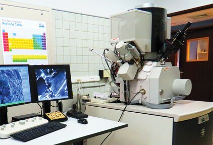
TEM/STEM - SEM
EMAT hosts
The former include two aberration corrected Titan cube instruments, the latter a dual beam and an environmental instrument.
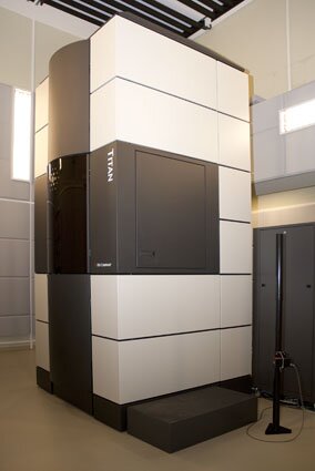
Thermo Fisher QU-Ant-EM
This unique instrument installed in June 2010 is one of the first double corrected instruments installed in Europe. Its double aberration correctors offer a 50 pm resolution in TEM and 70 pm in STEM. The instrument allows a flexible choice of acceleration voltage between 80 and 300kV to image a large range of materials. The presence of an X-Feg tip coupled to a Wien filter monochromator allows obtaining an electron probe with a very narrow energy dispersion of better than 140 meV.
It is equipped with a Quantum 966 Gatan Image Filter for electron energy loss spectroscopy and image filtering and can work in Dual-EELS mode for recording zero-loss and core-loss spectra quasi simultaneously. Two cameras are present at the end of the GIF. The US1000XP, mainly used for standard analysis, can record up to 1000 spectra/s in EELS. The K2 IS direct electron detector is dedicated to beam sensitive materials imaging and trace element detection in EELS. The presence of the IS module allows recording images up to 400 frames/s, which is especially interesting for in-situ experiments.
As an alternative to EELS, the instrument also offers an EDX system with an energy resolution of 136eV.
A rotatable biprism is available for electron holography and a Lorentz lens allows working in magnetic field free conditions.
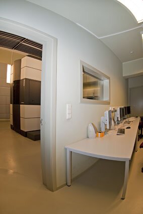
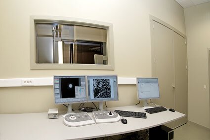
Automated software for 3D imaging in tomography and through focus series is available as well. The instrument is fully remote controlled from an operator room outside the shielded room of the microscope to improve the instrument stability.
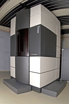
Thermo Fisher X-Ant-EM
This instrument, installed in March 2013, is especially equipped for spectroscopy techniques. Equipped with a D-Corr probe aberration corrector, this instrument offers a STEM resolution of 70 pm at 300 kV. Multiple STEM signals can be simultaneously recorded thanks to the presence of 4 independent detectors (HAADF, DF4, DF2, BF). The instrument allows a flexible choice of acceleration voltage between 60 and 300 kV, which is crucial for limiting the beam damage in beam sensitive materials (biological, polymers, ,..). The X-Feg tip, able to provide a high brightness and high current electron source, is coupled to a Wien-filter monochromator to provide an energy resolution in EELS better than 150 meV.
The X-Ant-TEM includes a GIF Enfinium spectrometer for electron energy loss spectroscopy. This spectrometer can record 1000 spectra/s and can work in Dual-EELS mode for recording zero-loss and core-loss spectra quasi simultaneously. In combination with the monochromator this offers unique opportunities for 2D/3D STEM atomic resolution mapping of elements and electronic properties. In combination with EELS, the instrument also offers a highly efficient SuperX system with a collection solid angle close to 1 sr. The high efficiency of this EDX detector allows to record atomic resolution EELS and EDX data simultaneously, up to 1000 spectra/s. This feature is ideal to map the atomic positions of both heavy and light atoms.
Two cameras are available in the microscope. The Gatan US1000XP offers good performances for standard TEM images and its improved acquisition speed allows good tracking during in-situ experiments. The Quantum Detectors Merlin camera, a direct electron detector able to reach 1200 full frames/s, is more dedicated to 4D STEM experiments, such as field mapping, electron diffraction and quantitative atom counting.
Automated software for 3D imaging in tomography is available as well. The instrument is fully remote controlled from an operator room outside the shielded room of the microscope to improve image stability.
Thermo Fisher Tecnai G2
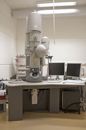
The Tecnai G2 (installed December 2008) is a versatile instrument that can be used for
- electron diffraction (SAED, CBED), phase and strain mapping thanks to the presence of the Nanomegas Digistar module for precession acquisition,
- high resolution transmission electron microscopy (HRTEM, point resolution 0.24nm, line resolution 0.102nm, 0.14nm information limit),
- high angle annular dark field scanning transmission electron microscopy (HAADF-STEM, 0.19nm lateral resolution)
- energy dispersive X-ray analysis.
Holders are available also for experiments at elevated and cryo temperatures, for tomography and for vacuum transfer of the samples from a glove box to the microscope column.
Tecnai Osiris
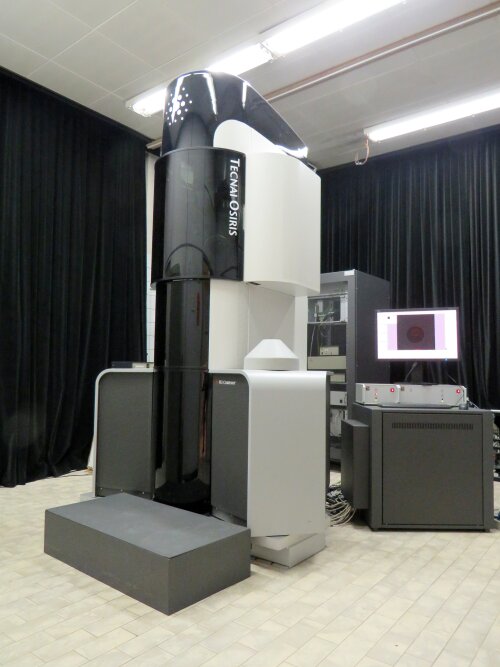
This microscope, installed in 2014, is equipped with a high brightness X-Feg electron gun which provides enhanced beam current as required for analytical work in STEM. The microscope is fitted with an analytical pole piece (6 mm pole piece gap), and provide STEM resolution down to 0.192 nm, and a TEM information limit of 0.14 nm. The extended pole piece gap allows the presence of a 4 quadrant Super X detector, especially designed to collect EDX signal over a large collection angle (0.7 sr). The position of these detectors, surrounding the sample area, allows acquiring quantifiable EDX signals even during a tomography series. A Gatan US1000XP CCD camera, allowing acquisitions with a few frames per second, is appreciated for in-situ work such as nano-indentation.
In addition the microscope is equipped with a post-column GIF 200 system for energy-loss spectroscopy and energy filtered imaging. A wide range of dedicated in-situ holders is available on this microscope (tomography, cooling, heating, gas and liquid experiments).
JEOL EM 3000 F
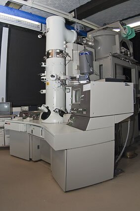
This FEG analytical resolution microscope (2002) equipped with FASTEM software combines high resolution imaging (0.191nm at Scherzer, 0.135nm information limit) with several analytical tools including an Inca EDX low-element microanalysis unit and a GIF2000 post column electron energy-loss spectrometer.
The STEM unit operating with a HAADF detector has a resolution of 0.136nm. A minimum probe size of 0.38nm in diameter can be obtained for spot analysis.
The computer controlled goniometer is equipped with an anti-drift piezostage and heating and cooling experiments can be performed.
JEOL 5590
Dedicated small scanning electron microscope (2003) with a tungsten filament, image resolution of 3.5 nm and equipped with an Inca EDX low-element microanalysis unit enabling surface morphology studies and identification of the elements present at the surface of conducting materials. Non-conducting materials require a coating with gold or carbon for optimal imaging. The instrument is mostly used for service work, rapid sample control and education purposes.
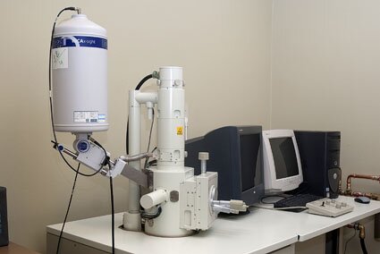
FEI QUANTA FEG 250
The Quanta 250 FEG is a field emission scanning electron microscope that can be operated at a broad range of pressures. As a result, the microscope can yield high-resolution images (with a spatial resolution of approximately 1 nm) in a saturated water vapour environment, keeping the sample in its native state. A Peltier cooled specimen stage furthermore enables one to switch easily between a hydrated and a non-hydrated phase of the specimen. The ability to operate the microscope at environmental conditions furthermore eliminates the need for conductive coating and will enable us to study surfaces of soft matter without any artefacts and obtain analytical information using the EDX or WDX system that is also available.
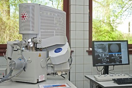
FEI Helios Nanolab 650
The Helios NanoLab 650 is a versatile, high-performance DualBeam system containing a Ga+ focused ion beam (FIB) (500eV - 30keV) together with a FEG extreme high resolution (XHR) scanning electron microscope (SEM) and Si-drift EDX detector for element analyses. This allows selective etching of materials while imaging the process and the area of interest at the same time with sub-nanometer resolution. In addition the system is equipped with a Gas Injection System (GIS) containing a Pt source and an Omniprobe for micro-manipulation of the specimen. The main purpose of the Helios 650 is high quality site-specific TEM specimen preparation with in-situ liftout. Also slice-and-view experiments can be performed.
