Since electrons only penetrate without too much energy spread through a maximum thickness of some hundred nanometer of solid material, samples for TEM have to be thinned to below this limit.
Thinning methods depend on the material and the observation mode:
Ion Milling
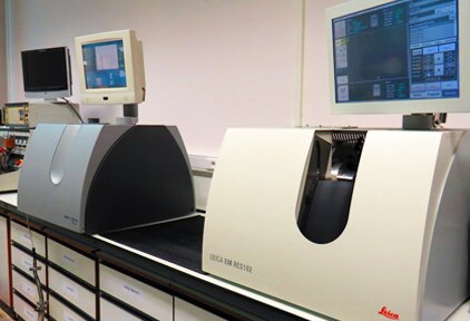
Non-conducting materials, such as ceramics or semiconductors, are thinned by ion milling after being mechanically polished to a thickness of 20µm. During ion milling, the sample is bombarded by accelerated Ar-ions. The different ion mills present are two Balzers RES 010 ion mills, a Gatan Duo Mill 600, a Baltec RES 101 and a Leica EM RES 102 instrument. With this procedure, plan view and cross-section samples can be prepared which are of particular interest for processed semiconductors, multilayers and coated materials.
Electropolishing
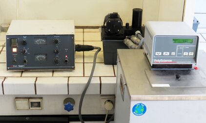
For conducting bulk materials, such as alloys or intermetallic compounds, electropolishing is by far the better technique. Different double jet Tenupol electropolishing machines are available in the laboratory.
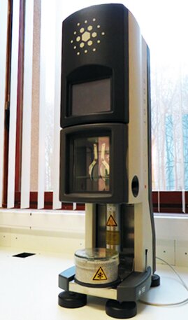
FEI Vitrobot Mark IV
The FEI Vitrobot Mark IV offers fully automated vitrification of particle suspensions (proteins, membranes, organelles, polymers, food and personal care products). It allows cryogenic TEM observation of these structures in their native state. The maximum specimen thickness for the plunging technique is about 1µm.
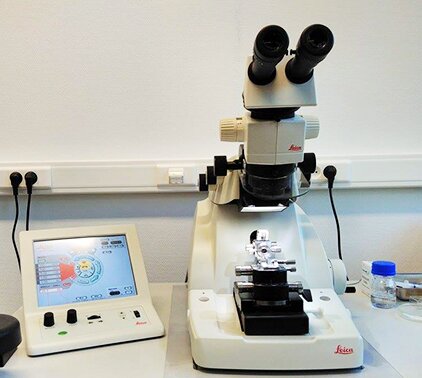
(Cryo)ultramicrotomy
Preparation of the TEM slices of soft materials can be done with (cryo)ultramicrotomy. The Leica EM UC7 ultramicrotome prepares industrial or biological semi- and ultra-thin sections (section thickness ranging from 30nm to 3µm), as well as perfectly smooth surfaces required for TEM and SEM examination. The Leica EM UC7 can be equipped with the Leica EM FC7 low temperature sectioning system, which enables the preparation of cryosections (-15°C to -185°C) for TEM (e.g. polymer sectioning).
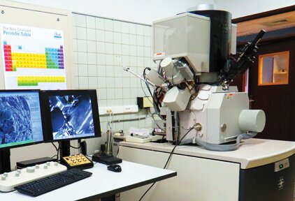
Dual beam focused ion beam microscopy (FIB)
When the original sample is too small for direct thinning, the Dual beam FIB/SEM Helios Nanolab 650 can be used. The latter instrument is also used for site-specific thinning of microsamples, the preparation of dedicated shapes for electron tomography, special TEM apertures (HAADF, electron vorteces, …), lithography, etc.
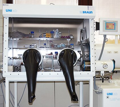
Working with O2 and H2O sensitive samples: Ar-filled Glove Box and Hermetically Closed Holder
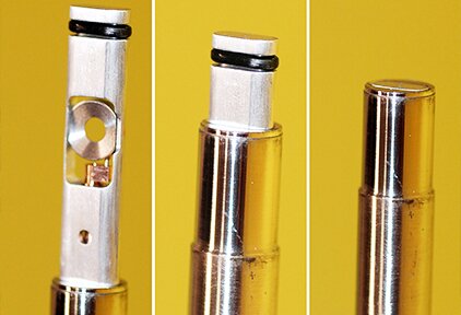
Many materials, such as metallic nanoparticles of electrodes for Li-ion batteries, can be handled only at the conditions preventing their interaction with air. Deposition of powders on the carbon-coated TEM grids and transportation of the sample to the microscope can be performed using an Ar-filled glove box and a dedicated hermetically closed holder under Ar atmosphere purified from O2 and H2O.
Sawing and mechanical polishing
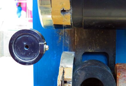
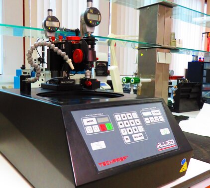
If necessary, the sample size is reduced to 1mm x 2.5mm pieces by using a high-precision saw (Struers Accutom-5) or a diamond wire saw (Well 3241). For a cross-section sample, two of these pieces are glued together with G1 (Gatan) epoxy. These pieces are subsequently mechanically polished to a thickness of 20µm by means of SiC polishing paper (Struers polisher) or diamond lapping films (Allied Multiprep). These thinned samples are subsequently thinned by ion milling.
In addition, it is possible to prepare wedge samples with the Allied Multiprep polishing system, or with the Allied tripod.
